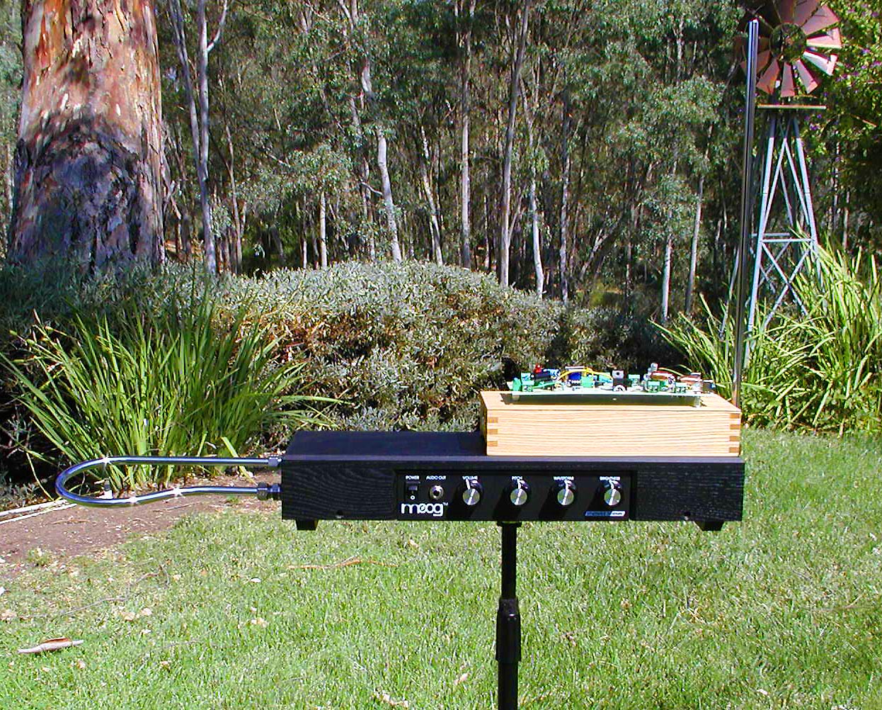
What is Q9 and associated circuitry (R41,C34) ? It is not on any of the Etherwave schematics I have found. It can be seen directly above CN1 connector.
Thank you.
What is Q9 and associated circuitry (R41,C34) ? It is not on any of the Etherwave schematics I have found. It can be seen directly above CN1 connector.
Thank you.
Hello Doug,
After a lot of eye strain it reveals itself as the Pitch Tuning section on the schematic working with Q5 near Q3 & Q4 the 2N3904 NPN Transistors as seen on many schematics . . . BUT Q9 2N3906 is a PNP configuration. I miss my theremin design days.
Your neighbor in Old Temecula CA
Christophe

Thanks for the input. This is what I am looking at. Q5 seems to be at the top, Q3 and Q4 to the left and Q9, whatever it is, is just to the right. I don't see Q9 on any schematic I have.
Interesting! I don't see any of these components on any schematics I have either. What is the date on the PCB?
R41 looks to be 2.2K and connects to one end of R6, though they might just be sharing a connection to -12V. If you could provide clear pictures of both sides of the PCB here we might be able to figure it out. Can you tell if Q9 is NPN or PNP? Is there any value printed on C34? What is that electrolytic to the left of C34?
The Q9 mystery needed its own post.
Will edit further if needed.
Transistor Q9 2N3906 PNP, C34 105 1uf, C9 330 COG, R4 2k2, R13 2k2, R12 10k, R39 10k, both Electrolytic 100uf
The Q9 base appears to be floating with No dc bias ? C34 1uf across emitter & base.
Oddly Q9 2N3906 PNP emitter goes to R39 then to pin 3 on the CN1 terminal which says -11v, pin 4 is gnd
Q9 collector goes directly to -12v, opposite board side term strip, interesting?
The neg side of cap 100uf goes directly to R41 2k2 which goes to -12v.
My guess Q9 is a thermal drift counter balance that did not work good so not documented. I also had a method where adjusting a potentiometer you could balance it out or even change the direction of the drift.
I have an EWS board in front of me, using eye loop. Board 11-211D
20 years ago you could grab a EWS with Moog Amp for $200 used, cheap when you consider theremin designers have well over $10,000 invested in the learning side of it all.

You must be logged in to post a reply. Please log in or register for a new account.